6.1 KiB
The TKey FPGA
Introduction
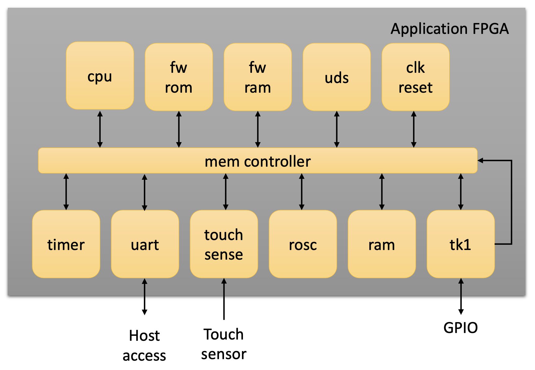
The TKey application FPGA (application_fpga design) contain the application platform CPU system onto which secure applications are loaded, measured and executed. The platform is a compact System on Chip (SoC) with the following cores.
The application FPGA is currently implemented using a Lattice iCE40 UltraPlus UP5K device. Only open tools are used in the toolchain.
Top level
The top level application_fpga design contain instances of all cores as well as the memory system. The memory system allows the CPU to access cores in different ways given the current exection mode. There are two execution modes - firmware and application. Basically, in application mode the access is more restrictive.
The API for all cores is described in the Memory mapped hardware functions in the System Description.
Cores
CPU
The CPU core is an instance of the PicoRV32 core. The instance enables the following features
- Compressed ISA (C extension)
- Fast multiplication. Two cycles for 32x32 multiplication
- Barrel shifter
No other modification to the core has been done. No interrupts are used.
Clock and reset
The device does not rely on external clock or reset. Instead the internal HFOSC oscillator combined with an internal PLL is used to generate the main clock. Currently the clock frequency driving the SoC is 18 MHz.
The device also generates its own reset.
FW ROM
The ROM memory containing the firmware. After reset the CPU will read from the ROM to load, measure and start applications.
The RAM memort is only accessible by the firmware.
FW RAM
A 512w32 small RAM only accessible by the firmware. The firmware use the RAM during loading and measurement of the application.
UDS
Unique Device Secret memory.
A 256 bit memory implemented using eight 32-bit registers. The registers can only be accessed once between power cycling. This means that the UDS must be read as u32. If read as u8, only the first byte from a given address will be correct, subsequent bytes will be zero.
The UDS can only be read in FW mode. Reading from the UDS in APP mode will return all zeros.
Application RAM
The 128 KByte main RAM. The RAM is only used by applications. The memory is cleared by firmware before an application is loaded.
The application RAM is available to use by firmware and applications.
Timer
A general purpose 32 bit timer. The timer will count down from the initial value to one. In order to handle long time sequences (minutes, hours, days) there is also a 32 bit prescaler.
The timer is available to use by firmware and applications.
UART
A standard UART interface for receiving bytes from and send bytes to the host via the interface MCU on the TKey.
The UART default speed is 62500 bps, but can be adjusted by the application. (Note that the host must set the same bitrate too.)
The UART contain a 512 but Rx-FIFO with status (data available).
The timer is available to use by firmware and applications.
ROSC
The ROSC is a ring oscillator based internal entropy source, or True Random Number Generator (TRNG). By default the TRNG use 32 free running digital oscillators. By default, the oscillators are sampled after 4096 cycles. The states are XOR combined to create a single bit. After another 4096 cycles a second bit is created, and the two bits are XOR combined to a single entropy bit. The entropy bit is added to a 32 bit entropy word.
After 32 bits has been collected, the data ready flag is set, indicating that an entropy word is ready for consumption. Note that entropy bit generation and collections is running continuously, bits will be added, and the discarded after 32 more bits have been added.
If a data word has been read from the TRNG, by default at least 32 bits will collected before new data will be available.
The ROSC TRNG is available to use by firmware and applications.
Note: The ROSC generates entropy with a fairly good quality. However for security related use cases, for example keys, the ROSC should not be used directly. Instead use it to create a seed for a Digital Random Bit Generator (DRBG), also known as a Cryptographically Safe Pseudo Random Number Generator (CSPRNG).
Examples of such generators are Hash_DRGG, CTR_DRBG, HKDF.
Touch sensor
The core provides a stable interface to the touch sensor on the TKey device. Using the core, the firmware and applications can get information about touch events and manage detection of events.
It is recommended that SW start by acknowledge any stray events prior to signal the user that a touch event is expected and then start waiting for an event.
The touch sensor is available to use by firmware and applications.
TKey
The TKey core contains several functions, and acts as main HW interface between firmware and applications. The core includes:
-
Read access to the 64 bit FPGA design name, expressed as ASCII chars.
-
Read access to the 32 bit FPGA design version, expressed as an integer
-
Control and status access for the RGB LED on TKey board
- Setting bit 0 high turns on the Blue LED.
- Setting bit 1 high turns on the Green LED.
- Setting bit 2 high turns on the Red LED.
-
Control and status access for the 4 GPIOs on the TKey board
-
GPIO 1 and 2 are inputs and provide read access to the current sampled value digital values on the pins.
-
GPIO 3 and 4 are outputs. The digital value written to the bits will be presented on the pins.
-
-
Application read access to information about the loaded application. The information is written by the firmware.
- Start address
- Size of address
-
Application read access to the CDI generated and written by the firmware when the application is loaded.
-
Application-Firmware execution mode control. Can be read by the application and written by firmware. When written to by the firmware, the hardware will switch to application mode and start executing the application.