11 KiB
Framing Protocol
Version
- Version: Draft 1.3
- 2021-12-20
1 Introduction
This document describes a proposal for a transport level communication protocol for the mta1_mkdf USB connected secure application device. The proposal describes the different endpoints, the different levels in the stack, framing and encoding.
2 System description and problem statement
The mta1_mkdf is a USB connected device. The device provides a secure compute platform and environment for applications providing some service and function to (the user of) the USB host. Examples of applications that can be implemented are AUTH token generators, Root of Trust, and signing oracles.
The mta1_mkdf is implemented using FPGA devices, and the computer functionality is based on RISC-V. Conceptually, the mta1_mkdf consists of three levels:
-
The hardware level. The actual FPGA devices and the hardware implemented in them, for example the RISC-V core, the application and data memories, but also timers, true random number generators and hardware access control.
-
The mta1_mkdf firmware and SDK level. The mta1_mkdf contains SW functionality (called firmware - FW) used to set up the application environment, but also provide the applications with things like host communication (the protocol described in this document), key generation, timers etc.
Similarly, the SDK provides similar convenience functions for the host side applications. Allowing host side applications to load applications on the mta1_mkdf, and then communicate with, use the applications running on the mta1_mkdf.
-
The applications running on the mta1_mkdf, the corresponding host SW.
The hardware, the FW as well as the applications can be endpoints with which programs on the host may communicate. This means that we need to be able to address different endpoints in the mta1_mkdf. And, crucially, the applications and their corresponding host SW may communicate using custom protocols that are not known today.
This means that we need a general transport mechanism for commands to, and responses from the endpoints in the mta1_mkdf. Due to the constrained environment the transport mechanism must be “light”, that is both easy to implement and to require few resources
2.1 mta1_mkdf system description details
The mta1_mkdf consists of two FPGA devices - interface_fpga and application_fpga.
The interface_fpga contains a USB core and FPGA-local control functionality (a Finite State Machine - FSM). The FSM is responsible for sending and receiving bytes to and from the application_fpga. Additionally, the FSM is the endpoint for commands directed to the HW in the interface_fpga. This allows the interface_fpga to provide functionality such as controlling the reset of the application_fpga, or provide host access to an entropy source.
The application_fpga contains FIFOs and control functionality needed to receive commands from the host (via the interface_fpga), and send back responses. The application_fpga also contains a System on Chip (SoC) with a PicoRV32 CPU core, memories for code and data storage. Additionally, the SoC includes functionality to provide a unique device secret (UDS), secure hashing, timers etc. Finally the application_fpga contains FW stored in read-only memory.
Figure 1 shows the high level architecture that illustrates the bidirectional data flows between the host and the interface_fpga. And then the separate command end response flows inside and between the FPGAs.
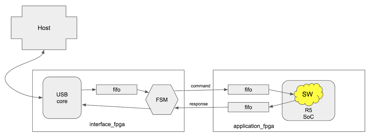
Figure 1: High level architecture with data flows.
Note that in the application_fpga it is FW and SW (application) that acts as endpoints, and they are responsible for interpreting commands and sending responses.
3 Protocol description
The communication is driven by the host and the protocol is command-response based. The host sends a command, and the mta1_mkdf must always send a response to a given command. Commands are processed by the mta1_mkdf in order. If the host sends a new command before receiving a response to the previous command, it is the responsibility of the host to determine to which command a received response belongs to.
Commands and responses are sent as frames with a constrained set of possible lengths. It is the endpoints that are communicating that decides what the data in the command and response frames mean, and if the commands and responses are valid and make sense.
3.1 Command frame format
A command frame consists of a single header byte followed by one or more data bytes. The number of data bytes in the frame is given by the header byte. The header byte also specifies the endpoint for the command.
The bits in the command header byte should be interpreted as:
-
Bit [7] (1 bit). Reserved - possible protocol version.
-
Bits [6..5] (2 bits). Frame ID tag.
-
Bits [4..3] (2 bits). Endpoint number.
- HW in interface_fpga
- HW in application_fpga
- FW in application_fpga
- SW (application) in application_fpga
-
Bit [2] (1 bit). Unused. MUST be zero.
-
Bits [1..0] (2 bits). Command data length.
- 1 byte
- 4 bytes
- 32 bytes
- 128 bytes
Note that the number of bytes indicated by the command data length field does not include the command header byte. This means that a complete command frame, with a header indicating a data length of 128 bytes, is 129 bytes in length.
Note that the host sets the frame ID tag. The ID tag in a given command MUST be preserved in the corresponding response to the command.
3.1.1 Command frame examples
Note that these examples mostly don't take into account that the first byte in the data (following the command header byte) typically is occupied by the particular app or FW command requested, so there is 1 byte less available for the "payload" of the command.
Some examples to clarify endpoints and commands:
-
0x00: A command to the HW in the interface_fpga with a single byte of data. The single byte could indicate action such as reading from the TRNG or resetting the application_fpga.
-
0x13: A command to the FW in the application_fpga with 128 bytes of data. The data could for example be parts of an application binary to be loaded into the program memory.
-
0x1a: A command to the application running in the application_fpga with 32 bytes of data. The data could be a 32 byte challenge to be signed using a private key derived in the mta1_mkdf.
3.2 Response frame format
A response consists of a single header byte followed by one or more bytes.
The bits in the response header byte should be interpreted as:
-
Bit [7] (1 bit). Reserved - possible protocol version.
-
Bits [6..5] (2 bits). Frame ID tag.
-
Bits [4..3] (2 bits). Endpoint number.
- HW in interface_fpga
- HW in application_fpga
- FW in application_fpga
- SW (application) in application_fpga
- Bit [2] (1 bit). Response status.
- OK
- Not OK (NOK)
- Bits [1..0] (2 bits). Response data length.
- 1 byte
- 4 bytes
- 32 bytes
- 128 bytes
Note that the number of bytes indicated by the response data length field does not include the response header byte. This means that a complete response frame, with a header indicating a data length of 128 bytes, is 129 bytes in length.
Note that the ID in a response MUST be the same ID as was present in the header of the command being responded to.
3.2.1 Response frame examples
Note that these examples mostly don't take into account that the first byte in the data (following the response header byte) typically is occupied by the particular app or FW response code, so there is 1 byte less available for the "payload" of the response.
-
0x01: A successful command to the HW in the interface_fpga, which responds with four bytes of data. For example the interface_fpga VERSION string.
-
0x14: An unsuccessful command to the FW in the application_fpga which responds with a single byte of data.
-
0x1b: A successful command to the application running in the application_fpga. The response contains 128 bytes of data, for example an EdDSA Ed25519 signature.
3.3 Command frame parsing and transfer
Commands are sent via USB to the interface_fpga. The Commands are buffered in the interface_fpga FIFO until the transfer_agent FSM is able to transfer the command to the correct endpoint (see Figure 1). To this end, the command header is parsed by the FSM in the interface_fpga to determine if the endpoint is in the interface_fpga itself, or if the command should be transferred to the application_fpga. Commands for the interface_fpga are processed by HW-functionality in the interface_fpga.
For commands to be transferred to the application, the transfer engine in the interface_fpga will interrogate the status of the application_fpga to determine that it can receive one or more bytes. If the application_fpga is capable of receiving the bytes, the transfer agent sends over the command bytes including the command byte to the application_fpga.
3.3 Response frame parsing and transfer
HW in the interface FPGA is responsible for detecting responses from any of the endpoints. If an endpoint has a response, the HW in the interface_fpga will extract the response and send it to the USB interface for delivery to the host. The HW in the interface_fpga will parse the response header bytes to determine how many bytes to expect.
For responses from the application_fpga, the HW in the interface_fpga will detect available bytes. When the HW in the interface_fpga is ready to send a response, it will extract bytes from the application_fpga and send them to the USB interface.
4 Inter-FPGA interface functionality
There are two communication directions between the FPGAs - with commands from the interface_fpga to the application_fpga, and with responses from the application_fpga to the interface_fpga. The important thing to note is that the directions are operated independently from each other.
4.1 transfer engines
The line interfaces used for each direction are identical and use the same design. But the direction and thus the transmitter and receiver are instantiated differently for each direction. This means that each FPGA contains one tx_engine and one rx_engine.
For commands the cmd_tx_engine is located in the interface_fpga, and the cmd_rx_engine is located in the application_fpga. For responses the response_tx_engine is located in the application_fpga, and the response_rx_engine is located in the interface_fpga.
4.2 Line interface
The line interface is a synchronous, byte oriented interface. Communication is driven by the tx_engine. Communication starts when the tx_engine has a byte to send, and the rx_engine indicates that it can receive a byte. The tx_engine sets the tx_en signal, starts running the tx_clk and shifts out the data bits in the byte to be transmitted. When all bits have been sent, the tx_engine must drop the en_signal for a cycle and check if the rx_engine is ready to receive a new byte.
Bits on the tx_data lines are updated by the tx_engine on the positive edge of the tx_clk. Bits are sampled by the rx_engine on the negative edge of the tx_clk. Bits are sent MSB first. The minimum number of wires, with a single tx_data wire is four. With two bit wide tx_data, the number of wires is five. This requires a total of 10 wires between the FPGAs. Figure 2 shows the ports including direction for the tx_engine and the rx_engine.

Figure 2: The tx_engine and the rx_engine with connections.
5. References
To Be Written.